Investigators: Usman Javed, Muhammad Wasif and Muhammad Sabieh Anwar
- Download complete details here in the form of Usman Javed’s dissertation.
- Download a description in the form of a Powerpoint presentation
Funding: LUMS grant FIF-PHY-2046
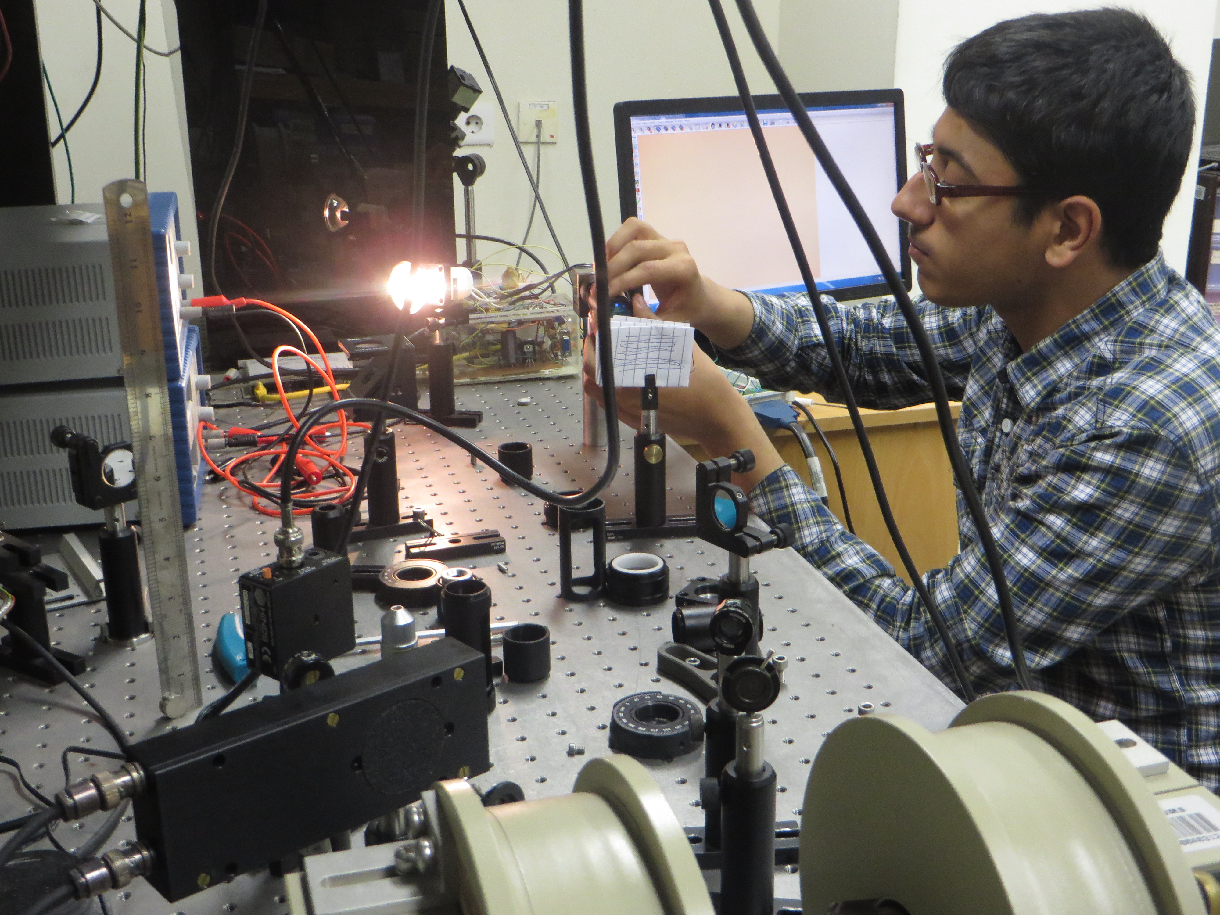
Physlab’s home grown atomic force microscope (AFM) is capable of resolving vertical features of the order of 20 nm. The AFM uses a nano-positioning actuator build from discarded piezoelectric discs, scavenged from piezo buzzers. The AFM analyzes surface topographic features by measuring the reflection of a laser beam off a cantilever making contact with the surface of the sample placed on a motorized transition stage driven by a motorized actuator. The reflected beam’s position is monitored by a closed loop proportional-integral control system that is specifically designed for this purpose. This AFM is a cost effective solution for a very sensitive instrument that has become essential in today’s research and development in nanotechnology, solid state physics, microbiology and many other fields of science and technology.
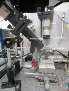
The AFM is built from commonly available components. The light source is a collimated and tightly focused diode laser, while detection and sensing is enabled by a multi-quadrant photodetector. The optical assembly is crafted on a mounting system and a CCD camera and illumination system is built for general optical microscopy. This helps in aligning the optics. Standard silicon nitride cantilevers affixed in clips are used to scan the sample. The mechanical assembly consists of a precision XYZ motion stage fitted with a Z axis picomotor. This picomotor has a nominal step size of 3 nm.
High precision, low noise, low drift amplification systems with output swings of 40 V on either side of zero, are designed to drive the piezo scanner. These amplifiers are thoroughly tested and calibrated. The power supplies for the system must also be low noise and low ripple. These circuits are an important feature of the AFM.
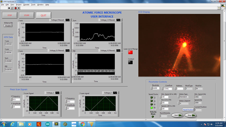
Finally the AFM has been equipped with a feedback control mechanism driven by a PID controller on an Arduino board with an ARM core microcontroller. The entire operation is controlled through a LabVIEW interface which is fully integrated and precisely synchronized with the controls of the nano-positioning actuator, picomotor and the Arduino board. A Labview based graphical user interface allows the user to fully control the instrument. Finally, the post-measurement image processing is performed through a free software Gwyddion.
Important specifications
- Best tested vertical resolution: approximately 20 nm
- X-Y resolution (pixel pitch): 12 nm (16 minutes scanning over the FOV) and 6 nm (32 minutes scanning over the FOV)
- Magnification: 600,000 x (calculated on a mesh sample, AFM-670 from Tedpella)
- field of view (FOV): 12 microns square
- Scan time: 16 minutes approx.
- Bandwidth: 500 Hz
- AFM mode: contact
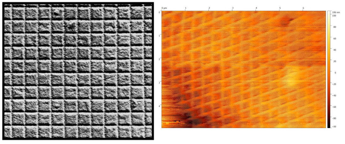
Micrograph of a cellulose acetate grid, with vertical pillars of height 30 nm and a spacing of 500 nm. The left shows the topopgraphy obtained from an electron microscope while the right shows the output from our AFM.
Three dimensional and two dimensional atomic force micrographs of DVD tracks.
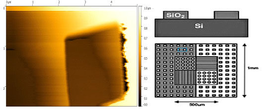
(a) Scan of 500 nm grooves in a callibration sample and (b) sample topology with the scan region marked with blue.
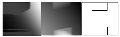
Image of two 500 nm pillars (a) without Control, (b) with control and (c) actual topology.
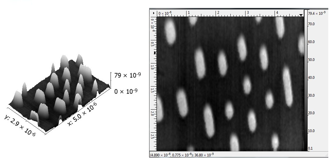
100 nm silicon nitride pillars scanned in feedback control mode.
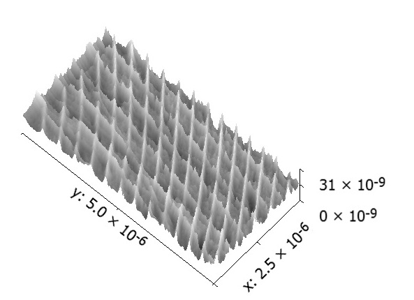
A three-dimensional view of the 30 nm cellulose acetate grid shown above.
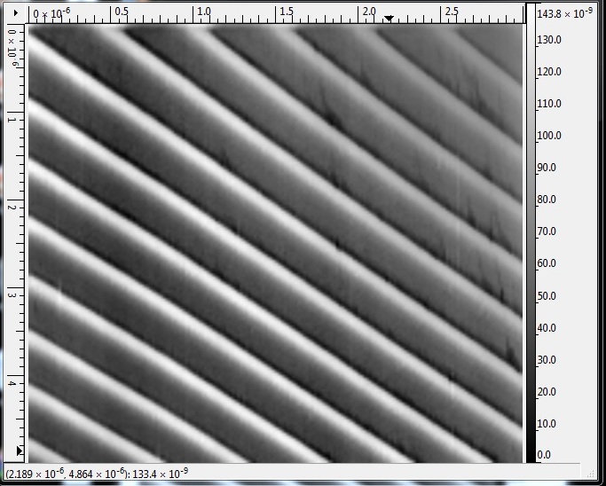
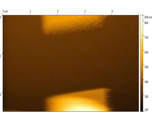
AFM of a blank writeable DVD.